Final
We have reached the last step and just need to connect our blocks together. We now have a fully functional processor that is capable of running programs we have written ourselves.
In the source code you can see the assign statements that realize the multiplexers we saw on the microarchitecture. The module has two input signals (clk, rst) which, if we wanted to realize the chip, would come from outside the processor. Usually a clock generator is placed on a board which serves as input for the processor, the reset signal could be e.g. a button on a board with which we can reset the processor.
Critical Path
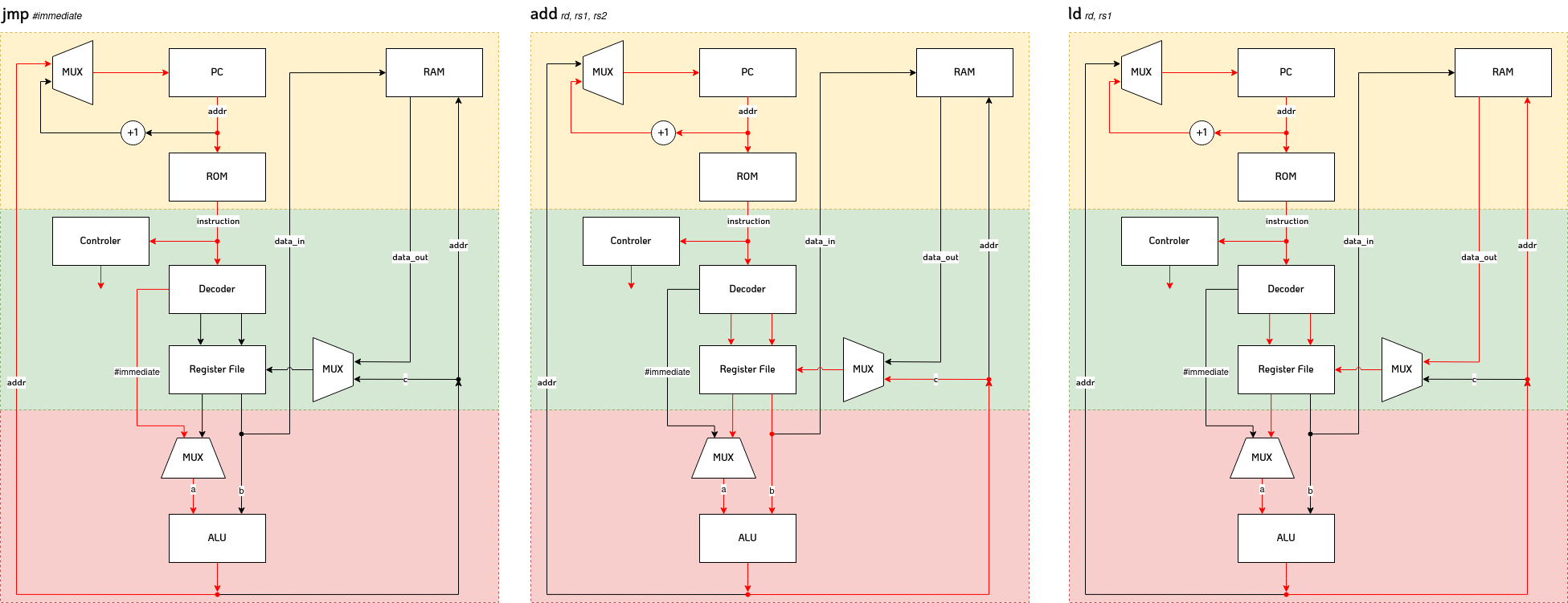
To get a feeling for the execution of an instruction, we will show the critical paths (in red) of three instructions (jmp, add, ld). By critical path in this context, we mean the paths that are crucial for the instructions and emphasize the data flow.
As we can see in the diagrams below, the critical path is different according to the instruction. In the case of the jmp instruction, for example, the new address for the PC register is loaded as an immediate value via the ALU. In the case of the add instruction, the result of the ALU is loaded into the register file and into the addressed target register. In the case of the ld instruction, the output of the ALU is used as the address for a memory access. The corresponding byte is then loaded into the target register. The data flow is directed by the controller.
Donate (Bitcoin & Lightning)
Choose Payment Method


Copyright ©. All Rights Reserved. — Designed by Bitspinner